- 您现在的位置:买卖IC网 > Sheet目录310 > AL5801W6-7 (Diodes Inc)IC LED DRVR HIGH BRIGHT 26SOT
AL5801
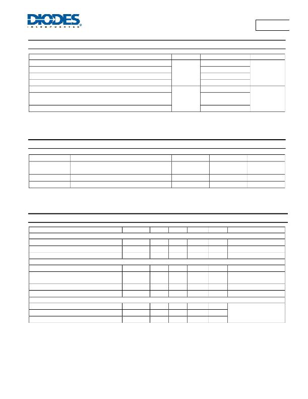
Package Thermal Data
Characteristic
Power Dissipation (Note 5) @ T A = +25°C
Power Dissipation (Note 6) @ T A = +25°C
Power Dissipation (Note 7) @ T A = +25°C
Power Dissipation (Note 8) @ T A = +25°C
Thermal Resistance, Junction to Ambient Air (Note 5) @ T A = +25°C
Thermal Resistance, Junction to Ambient Air (Note 6) @ T A = +25°C
Thermal Resistance, Junction to Ambient Air (Note 7) @ T A = +25°C
Thermal Resistance, Junction to Ambient Air (Note 8) @ T A = +25°C
Notes:
5. Device mounted on 15mm x 15mm 2oz copper board.
Symbol
P D
R θ JA
Value
0.75
0.70
0.85
1.05
165
180
145
120
Unit
W
°C/W
6. Device mounted on 25mm x 25mm 1oz copper board.
7. Device mounted on 25mm x 25mm 2oz copper board.
8. Device mounted on 50mm x 50mm 2oz copper board.
Recommended Operating Conditions (@T A = +25°C, unless otherwise specified.)
Symbol
V BIAS
V OUT
I LED
T A
Parameter
Supply voltage range
OUT voltage range
LED pin current (Note 9)
Operating ambient temperature range
Min
3.5
1.1
25
-40
Max
20
100
350
125
Unit
V
mA
°C
Note:
9. Subject to ambient temperature, power dissipation and PCB.
NMOSFET Electrical Characteristics: (Q1) (@T A = +25°C, unless otherwise specified.)
Characteristic
Symbol
Min
Typ
Max
Unit
Test Condition
OFF CHARACTERISTICS
Drain-Source Breakdown Voltage
Zero Gate Voltage Drain Current
Gate-Source Leakage
BV DSS
I DSS
I GSS
100
?
?
?
?
?
?
1
± 100
V
μA
nA
V GS = 0V, I D = 250μA
V DS = 60V, V GS = 0V
V GS = ± 20V, V DS = 0V
ON CHARACTERISTICS
Gate Threshold Voltage
Static Drain-Source On-Resistance
Forward Transconductance
Diode Forward Voltage
V GS(th)
R DS (ON)
g fs
V SD
2.0
?
?
?
?
?
?
0.9
0.89
4.1
0.85
0.99
?
1.1
V
Ω
S
V
V DS = V GS , I D = 250μA
V GS = 10V, I D = 1.5A
V GS = 6V, I D = 1A
V DS = 15V, I D = 1A
V GS = 0V, I S = 1.5A
DYNAMIC CHARACTERISTICS
Input Capacitance
C iss
?
129
?
pF
Output Capacitance
Reverse Transfer Capacitance
C oss
C rss
?
?
14
8
?
?
pF
pF
V DS = 50V, V GS = 0V
f = 1.0MHz
AL5801
Document number: DS35555 Rev. 3 - 2
3 of 11
www.diodes.com
July 2012
? Diodes Incorporated
发布紧急采购,3分钟左右您将得到回复。
相关PDF资料
AL5802-7
IC LED DRVR LINEAR 30V SOT26
AL8400SE-7
IC CTRLR LED DRIVER SOT353
AL8805W5-7
IC REG SW CONV BUCK ASYNC SOT-23
AL8806MP8-13
IC LED DVR CONS CURR 8MSOP
AL8807W5-7
IC LED DRVR DCDC BUCK SOT25
AL9910AS-13
IC LED DRVR HIGH BRIGHT SO8EP
ALC60481R05
PWR SUP AC-DC 6-48V 1.05A 50.4W
ALV100362R5
POWER SUPPLY AC-DC 36V 2.5A 90W
相关代理商/技术参数
AL5801W6Q-7
制造商:Diodes Incorporated 功能描述:DISCRETE LED DRIVER SOT26 T&R 3K - Tape and Reel
AL5802
制造商:DIODES 制造商全称:Diodes Incorporated 功能描述:30V, ADJUSTABLE CURRENT SINK LINEAR LED DRIVER
AL5802-7
功能描述:LED照明驱动器 Discrete LED Driver Driver,SOT26,3K
RoHS:否 制造商:STMicroelectronics 输入电压:11.5 V to 23 V 工作频率: 最大电源电流:1.7 mA 输出电流: 最大工作温度: 安装风格:SMD/SMT 封装 / 箱体:SO-16N
AL5802EV1
功能描述:AL5802 1, Non-Isolated Output LED Driver Evaluation Board 制造商:diodes incorporated 系列:- 零件状态:有效 电流 - 输出/通道:120mA 输出和类型:1,非隔离 电压 - 输出:- 特性:- 电压 - 输入:4.5 V ~ 30 V 所含物品:板 使用的 IC/零件:AL5802 标准包装:1
AL5802LP4-7
功能描述:LED 驱动器 IC 1 输出 线性 PWM 调光 100mA X2-DFN1310-6 制造商:diodes incorporated 系列:- 包装:剪切带(CT) 零件状态:有效 类型:线性 拓扑:- 内部开关:是 输出数:1 电压 - 供电(最低):4.5V 电压 -?供电(最高):30V 电压 - 输出:30V 电流 - 输出/通道:100mA 频率:- 调光:PWM 应用:标牌 工作温度:-40°C ~ 125°C(TA) 安装类型:表面贴装 封装/外壳:6-XFDFN 裸露焊盘 供应商器件封装:X2-DFN1310-6 标准包装:1
AL5802LP-7
功能描述:LED 驱动器 IC 1 输出 线性 PWM 调光 150mA U-DFN1616-6 制造商:diodes incorporated 系列:- 包装:剪切带(CT) 零件状态:有效 类型:线性 拓扑:- 内部开关:是 输出数:1 电压 - 供电(最低):4.5V 电压 -?供电(最高):30V 电压 - 输出:30V 电流 - 输出/通道:150mA 频率:- 调光:PWM 应用:标牌 工作温度:-40°C ~ 125°C(TA) 安装类型:表面贴装 封装/外壳:6-XFDFN 裸露焊盘 供应商器件封装:U-DFN1616-6 标准包装:1
AL5802LPL-7
功能描述:FUNCTIONAL ARRAY U-DFN3030-6 T&R 制造商:diodes incorporated 系列:* 零件状态:有效 标准包装:3,000
AL5802QW6-7
功能描述:LED 驱动器 IC 1 输出 线性 PWM 调光 120mA SOT-26 制造商:diodes incorporated 系列:- 包装:剪切带(CT) 零件状态:过期 类型:线性 拓扑:- 内部开关:是 输出数:1 电压 - 供电(最低):4.5V 电压 -?供电(最高):30V 电压 - 输出:0.8 V ~ 30 V 电流 - 输出/通道:120mA 频率:- 调光:PWM 应用:标牌 工作温度:-40°C ~ 125°C(TA) 安装类型:表面贴装 封装/外壳:SOT-23-6 供应商器件封装:SOT-26 标准包装:1
